One of the crucial keys to solid state electronics is the nature of the P-N junction. When p-type and n-type materials are placed in contact with each other, the junction behaves very differently than either type of material alone. Specifically, current will flow readily in one direction (forward biased) but not in the other (reverse biased), creating the basic diode. This non-reversing behavior arises from the nature of the charge transport process in the two types of materials.
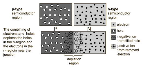
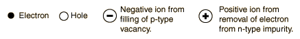
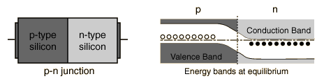 The open circles on the left side of the junction above represent "holes" or deficiencies of electrons in the lattice which can act like positive charge carriers. The solid circles on the right of the junction represent the available electrons from the n-type dopant. Near the junction, electrons diffuse across to combine with holes, creating a "depletion region". The energy level sketch above right is a way to visualize the equilibrium condition of the P-N junction. The upward direction in the diagram represents increasing electron energy.
Depletion Region
When a p-n junction is formed, some of the free electrons in the n-region diffuse across the junction and combine with holes to form negative ions. In so doing they leave behind positive ions at the donor impurity sites.
Depletion Region Details
 | In the p-type region there are holes from the acceptor impurities and in the n-type region there are extra electrons. |
 | When a p-n junction is formed, some of the electrons from the n-region which have reached the conduction band are free to diffuse across the junction and combine with holes. |
 | Filling a hole makes a negative ion and leaves behind a positive ion on the n-side. A space charge builds up, creating a depletion region which inhibits any further electron transfer unless it is helped by putting a forward bias on the junction. |
 Bias effect on electrons in depletion zone
 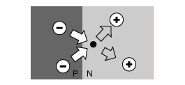 Equilibrium of junction Coulomb force from ions prevents further migration across the p-n junction. The electrons which had migrated across from the N to the P region in the forming of the depletion layer have now reached equilibrium. Other electrons from the N region cannot migrate because they are repelled by the negative ions in the P region and attracted by the positive ions in the N region.
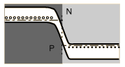
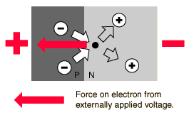
 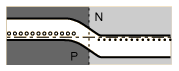 Reverse bias An applied voltage with the indicated polarity further impedes the flow of electrons across the junction. For conduction in the device, electrons from the N region must move to the junction and combine with holes in the P region. A reverse voltage drives the electrons away from the junction, preventing conduction.
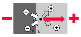 Forward bias An applied voltage in the forward direction as indicated assists electrons in overcoming the coulomb barrier of the space charge in depletion region. Electrons will flow with very small resistance in the forward direction.
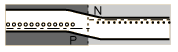
Fuente:http://hyperphysics.phy-astr.gsu.edu/hbase/solids/pnjun.html
Nombre: Lenny Ramirez
Asignatura: EES
Invite your mail contacts to join your friends list with Windows Live Spaces. It's easy!
Try it!
No hay comentarios:
Publicar un comentario