A silicon crystal is different from an insulator because at any temperature above absolute zero temperature, there is a finite probability that an electron in the lattice will be knocked loose from its position, leaving behind an electron deficiency called a "hole".
If a voltage is applied, then both the electron and the hole can contribute to a small current flow.
The conductivity of a semiconductor can be modeled in terms of the band theory of solids. The band model of a semiconductor suggests that at ordinary temperatures there is a finite possibility that electrons can reach the conduction band and contribute to electrical conduction.
The term intrinsic here distinguishes between the properties of pure "intrinsic" silicon and the dramatically different properties of doped n-type or p-type semiconductors. |
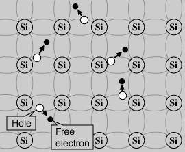
Semiconductor Current
Both electrons and holes contribute to current flow in an intrinsic semiconductor. 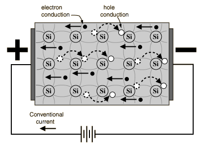
Semiconductor Current
The current which will flow in an intrinsic semiconductor consists of both electron and hole current. That is, the electrons which have been freed from their lattice positions into the conduction band can move through the material. In addition, other electrons can hop between lattice positions to fill the vacancies left by the freed electrons. This additional mechanism is called hole conduction because it is as if the holes are migrating across the material in the direction opposite to the free electron movement. The current flow in an intrinsic semiconductor is influenced by the density of energy states which in turn influences the electron density in the conduction band. This current is highly temperature dependent. 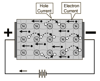
Electrons and Holes
In an intrinsic semiconductor like silicon at temperatures above absolute zero, there will be some electrons which are excited across the band gap into the conduction band and which can produce current. When the electron in pure silicon crosses the gap, it leaves behind an electron vacancy or "hole" in the regular silicon lattice. Under the influence of an external voltage, both the electron and the hole can move across the material. In an n-type semiconductor, the dopant contributes extra electrons, dramatically increasing the conductivity. In a p-type semiconductor, the dopant produces extra vacancies or holes, which likewise increase the conductivity. It is however the behavior of the p-n junction which is the key to the enormous variety of solid-state electronic devices. 
Nombre: Lenny Ramirez
Asignatura:EES
Discover the new Windows Vista
Learn more!


No hay comentarios:
Publicar un comentario